
Regular practice with AP Inter 2nd Year Physics Study Material Chapter 14 Semiconductor Devices Questions and Answers helps students stay prepared for examinations.
AP Inter 2nd Year Physics 14th Lesson Semiconductor Devices Questions and Answers
I. Multiple Choice Questions
Question 1.
Following is an example of a compound semiconductor [ ]
1) Al2O3
2) SiO2
3) H2O
4) GaAs
Answer:
4) GaAs
Gallium Arsenide (Ga As) is classified as a compound semiconductor
Question 2.
Which of the following is used as pentavalent impurities for doping process?[ ]
1) Arsenic
2) Boron
3) Indium
4) Aluminium
Answer:
1) Arsenic
Arsenic is used as a Pentavalent depend because, it contributes a base electron to the semi conductor lattice, creating an n-type material with high increased electrical conductivity.
Question 3.
For an n-type semiconductor ne = number of conduction electrons and nh, = number of holes, then ____. [ ]
1) ne = nh
2) ne > nh
3) ne < nh
4) ne = (nh/2)
Answer:
2) ne > nh
For n-type semiconductor, ne > nr, because the material is intentionally doped with pentavalent impurities.
Question 4.
The energy band gaps of silicon and germanium are [ ]
1) 0.7eV, 1.1eV
2) 1eV, 0.7eV
3) 1.1eV,0.7eV
4) 2eV, 1.5eV
Answer:
3) 1.1eV,0.7eV
Silicon and Germanium have different atomic sizes, nuclear charges and crystal binding forces. Because of this it takes 1.1 ev of energy the break a covalent bond in Silicon, compared to only 0.7ev in Germanium.
Question 5.
On the basis of electrical conductivity, which one of the following material has the smallest resistivity? [ ]
1) Germanium
2) Silicon
3) Glass
4) Silver
Answer:
4) Silver
Silver has lowest resistivity 1.59 × 10⁻⁸Ω. It is due to its unique atomic structure how electronegativity, high concentration of free electrons.
Question 6.
In case of full wave rectification, if the input frequency is 60 Hz, then the output frequency would be [ ]
1) 60 Hz
2) 120 Hz
3) 100 Hz
4) 150 Hz
Answer:
2) 120 Hz
In a full wave rectifier the input frequency n = 60 Hz then its output frequency is 2n = 120 Hz

Question 7.
The electron concentration in an n-type semiconductor is the same as hole concentration in a p-type semiconductor. An external field (electric) is applied across each of them. Compare the currents in them. [ ]
1) No current will flow in p-type, current will only flow in n-type
2) Current in n-type = Current in p-type
3) Current in p-type > Current in n-type
4) Current in n-type > Current in p-type
Answer:
4) Current in n-type > Current in p-type
In > Ip. At equal charge carrier concentration, current in entire (mobility of electrons) is higher than current in p-type (mobility of holes)
Question 8.
For a p-n junction diode, the current in reverse bias is in the order of [ ]
1) Few mA
2) Few amperes
3) Few µA
4) Few kilo amperes
Answer:
3) Few µA
In a p-n junction diode, the reverse bias current is extremely small in the order of µA for Ge
Question 9.
The increase in the width of the depletion region in a p-n junction diode is due to [ ]
1) reverse bias only
2) both forward bias and reverse bias
3) high doping concentrations
4) forward bias only
Answer:
1) reverse bias only
The increase in the width of the depletion region in a p-n junction diode is due to reverse bias only
Question 10.
A Ge specimen is doped with aluminium. The concentration of acceptor atoms is 1021 atoms/m3. Given that the intrinsic concentration of electrons in the specimen is 1019/m3. The new electron concentration is [ ]
1) 1017/m3
2) 1018m3
3) 104/m3
4) 102/m3
Answer:
1) 1017/m3
When concentration of electron is n, hole is p and inter intrinsic carrier is n; then nP = \(\mathrm{n}_{\mathrm{i}}^2\)
∴ n = \(\frac{\mathrm{n}_{\mathrm{i}}^2}{\mathrm{P}}\) = \(\frac{\left(10^{19}\right)^2}{10^2}\) = \($\frac{10^{38}}{10^{21}}$\) = 1017m3
Question 11.
Which of the following circuits represents a forward biased diode? [ ]
Choose the correct answer from the options given below:
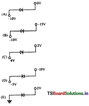
1) (C) and (E) only
2) (A) and (D) only
3) (B), (D) and (E) only
4) (B), (C) and (E) only
Answer:
4) (B), (C) and (E) only
A diode in forward biased, Vanode > Vcathode. Among the given (B)(C) (E) are correct.
II. Fill in the Blanks
Question 1.
In a vacuum tube, the electrons are supplied by a ___.
Answer:
cathode
In a vacuum tube, the electrons are supplied by a cathode.
Question 2.
In vacuum tubes, electrons flow from the cathode to the anode in ___ direction.
Answer:
only one
In vacuum tubes, electrons flow from the cathode to the anode in only one direction.
Question 3.
The conduction in a semiconductor possible due to motion of ___ in the conduction band and ___ in the valence band.
Answer:
The conduction in a semiconductor possible due to motion of electrons in the conduction band and holes in the valence band.
Question 4.
The gap between the top of the valence band. and bottom of the conduction band is called the ____.
Answer:
energy band gap/forbidden energy gap.
The gap between the top of the valence band and bottom of the conduction band is called the energy band gap/forbidden energy gap.
Question 5.
The semiconductor elements Ge and Si crystal structure is almost similar to ____ structure.
Answer:
diamond cubic crystal
The semiconductor elements Ge and Si crystal structure is almost similar to diamond cubic crystal structure.
Question 6.
In intrinsic semiconductors, the number of free electrons(ne) = number of holes (nh) = ni where ni is called ____.
Answer:
intrinsic carrier concentration
In intrinsic semiconductors, the number of free electrons(ne) = number of holes (nh) = ni where ni is called intrinsic carrier concentration.
Question 7.
The pentavalent dopant donates one extra electron for conduction and hence this impurity is called ___.
Answer:
donor
The pentavalent dopant donates one extra electron for conduction and hence this impurity is called donor.
Question 8.
In an n-type Si semiconductor, the donor energy level ED is slightly ___ the bottom of the conduction band (EC).
Answer:
below
In an n-type Si semiconductor, the donor energy level ED is slightly below the bottom of the conduction band (EC).
Question 9.
At Thermal equilibrium the electron and hole Concentration in an intrinsic semiconductor is ___.
Answer:
equal.
At Thermal equilibrium the electron and hole Concentration in an intrinsic semiconductor is equal.
Question 10.
In the p-n juñction diode symbol, the direction of arrow indicates ____.
Answer:
direction of conventional current
In the p-n junction diode symbol, the direction of arrow indicates direction of conventional current.
III. One Word Answer Questions
Question 1.
At what temperature the intrinsic semiconductor will behave like an insulator?
Answer:
At absolute zero temperature (0 K) intrinsic semi conductor behaves like an insulator
Question 2.
What is the ratio of number of holes and the number of conduction electrons in an intrinsic semiconductor?
Answer:
The ratio of the number of holes (nh) to the number of conduction electrons (ne) in an intrinsic semiconductor is 1:1.
Question 3.
What is the overall charge of the p-type semiconductor crystal?
Answer:
The overall charge of p-type semi conductor crystal is electrically neutral (zero).
Question 4.
Draw the circuit symbol of the p-n junction diode.
Answer:
Circuit symbol of the p-n junction diode: 

Question 5.
For a p-n junction diode, built in potential = V0 and applied voltage is V (V >V0) and diode is in forward bias then what is the height of effective barrier?
Answer:
The effective barrier height = V0 – V.
The effective barrier height (potential) of a forward biased diode is reduced by the applied voltage (V) from initial voltage (V0).
Question 6.
What is the forbidden energy gap in Ge semiconductor crystal in terms of Joules?
Answer:
Forbidden energy gap in Ge at room temperature Eg = 0.72 × 1.6 × 10-19 J = 1.15 × 10⁻¹⁹ J
Question 7.
What is the ngme of the current due to motion of charge carriers when external electric field is applied.
Answer:
The current produced by the motion of charge carries under the influence of an external electric field is known as drift current.
Question 8.
At thermal equilibrium condition what will be the product of number of electrons and number of holes in any semiconductor material?
Answer:
At thermal equilibrium, the product of the concentration of electrons (ne) and the concentration of holes (nh) in any semi conductor material is given by nenh = \(\mathbf{n}_{\mathbf{i}}^2\).
Here ni is the intrinsic carrier concentration.
This is known as the “Law of mass Action”.
Question 9.
What is the energy band which includes the energy levels of the valence electrons?
Answer:
The valence band is the energy band includes the energy levels of the valence electrons. It is the highest occupied energy band in a material.
Question 10.
What is the name of the process “adding impurities to the intrinsic semiconductor to make extrinsic semiconductor”?
Answer:
Doping is the process of adding impurities to an intrinsic semiconductor to make extrinsic semi conductor.
Question 11.
The output voltage in the following circuit is (Consider diodes are ideal)
Answer:
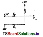
Output voltage is equal to zero.
Reason: The diode D2 conducts and acts as a short circuit to ground.
Question 12.
What is the output frequency of a half-wave rectifier if the input voltage frequency is 50 Hz?
Answer:
If the input is 50Hz, out is also 50Hz.
Reason: The output frequency of a rectifier is equal to input voltage frequency.
Question 13.
What is the current through an ideal p-n junction diode shown in the following figure.
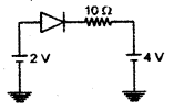
Answer:
Current through the diode is i = 0 A.
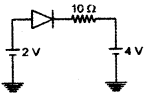
Reason: For an ideal P-N junction diode in reverse bias, the resistance is considered infinite and hence no current flows through it.
Question 14.
A semiconductor is known to have an electron concentration of 8 × 10¹³ /cm3 and a hole concentration 5 × 10/cm3. What type of the semiconductor is it?
Answer:
It is an n-type semiconductor because ne > nh.
Electron concentration ne = 8 × 10¹³ /cm3 ; Hole concentration nh = 5 × 10² /cm3. Here the electron concentration is much higher than the hole concentration.
IV. Very Short Answer Questions
Question 1.
What are intrinsic and extrinsic semiconductors ?
Answer:
Intrinsic Semiconductor:
Pure semiconductor like silicon is called intrinsic semiconductor.
In an intrinsic semiconductor, number of electrons(ne) = number of holes(nh).
Extrinsic Semiconductor : A semiconductor doped with trivalent or pentavalent impurity is called extrinsic semiconductor.
Extrinsic semiconductors are of two types,
- n-type semiconductor and
- p-type semiconductor.
Question 2.
What is an n-type semiconductor?
What are the majority and minority charge carriers in it?
Answer:
n-type Semiconductor:
Silicon or Germanium doped with pentavalent impurity like Arsenic is called n-type semiconductor. The pentavalent atoms add extra electrons and make it n-type semiconductor.
In n-type semiconductor, majority charge carriers are electrons and minority charge carriers are holes.
Question 3.
What is a p-type semiconductor ? What are the majority and minority charge carriers in it?
Answer:
p-type Semiconductor:
Silicon or Germanium doped with trivalent impurity like Indium is called p-type semiconductor. The trivalent atoms add extra holes and make it p-type semiconductor.
In p-type semiconductor, majority charge carriers are holes and minority charge carriers are electrons.
Question 4.
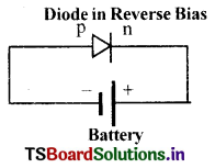
How is a battery connected to a junction diode in
(1) forward and
(2) reverse bias?
Diode in Forward Bias
Answer:
1) Forward bias:
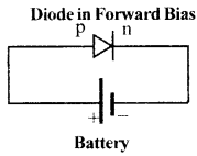
In forward bias, a battery is connected to the diode such that its positive terminal is towards p-end of diode.
2) Reverse bias:
In reverse bias, a battery is connected to the diode such that its positive terminal is towards n-end of diode.
Question 5.
What do you mean by donor impurity and acceptor impurity?
Answer:
Donor impurities are atoms with five valence electrons-like Phosphorus (Pentavalent) added to semiconductors to donate free electrons forming n-type materials.
Acceptor impurities are atoms with three valence electrons- like Boron (trivalent) added to semiconductors to create vacancies (holes) forming p-type materials.
Question 6.
What is reverse saturation current of p-n junction diode?
Answer:
Reverse saturation current is the small amount of current that flows through a p-n junction diode when it is reverse biased. It is caused by the flow of minority carriers.
Question 7.
Define depletion layer and what is the breakdown voltage of p-n junction diode.
Answer:
Depletion layer: It is the narrow region on either side of the p-n junction which is free from mobile charge carriers.
Breakdown voltage: It is the voltage in a reverse biased p-n junction at which the current suddenly rises to a large values.
Question 8.
What happens to the width of the depletion layer in a p-n junction diode when it is
- forward-biased and
- reverse biased?
Answer:
- In forward bias, the width of the depletion layer of a diode decreases
- In reverse bias, the width of the depletion layer of a diode increases.
Question 9.
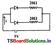
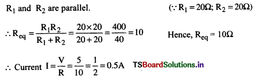
What is the current through the battery in the circuit as shown in figure, here diodes are ideal?
Answer:
Both the diodes are in forward bias and both are ideal.
Question 10.
What is rectification? Which device is used as rectifier?
Answer:
Rectification is the process of converting an alternating current in to direct current.
The device used for this rectification process is called a rectifier.
V. Short Answer Questions
Question 1.
Describe energy band diagram of intrinsic semiconductors at 0 K.
Answer:
Intrinsic semiconductors:
Intrinsic semiconductors are made up of pure form of semi conductor. These atoms are tetravalent.
They behave like insulators at OK.
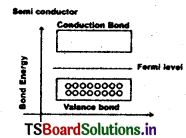
At 0K, the valence band is completely filled with electrons and conduction band is empty.
Thus there are no free electrons to conduct electricity. Hence they act as insulators at 0K.
At 0K there is a small energy gap between the top of the valence band and the bottom of the conduction band. Since, no thermal energy is available at 0 K, no electrons can jump across this gap.
At higher temperatures (T > 0K) thermal energy excites some electrons from valence band to the conduction band and leaving equal number of holes there.
Question 2.
How conductors, insulators and semiconductors are classified based on the energy band diagram?
Answer:
1) Conductors: In conductors, the conduction band and the valence band overlap or are very close to each other. Conduction band is partially filled, and there is no forbidden energy gap (band gap) between the valence band and conduction band. This allows electrons to move freely, resulting in high electrical conductivity.
2) Insulators: In insulators, the valence band is completely filled, and the conduction band is empty. There is a large forbidden energy gap (Eg > 3eV) between the valence band and conduction band. This large gap prevents electrons from jumping to the conduction band resulting in very low electrical conductivity.
3) Semiconductors: In semiconductors, the valence band is also filled, but the conduction band is either empty or partially filled. The forbidden energy gap is very small (Eg < 3eV). This smaller gap allows some electrons to jump into the conduction band due to thermal excitation, resulting in moderate electrical conductivity.
Question 3.
What are n-type and p-type semiconductors? Explain the process of formation of p-n junction diode.
Answer:
n-type Semiconductor. Silicon or germanium doped with pentavalent impurity like arsenic is called n-type semiconductor. The pentavalent atoms add extra electrons and make it n-type semiconductor. In n-type semiconductor, majority charge carriers are electrons and minority charge carriers are holes.
p-type Semiconductor: Silicon or germanium doped with trivalent impurity like indium is called p-type semiconductor. The trivalent atoms add extra hole’s and make it p-type semiconductor. In p-type semiconductor, majority charge carriers are holes and minority charge carriers are electrons.
Process of formation of p-n junction diode:
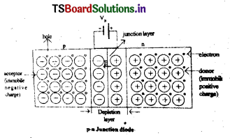
When a semiconductor material such as silicon or Germanium crystal is doped such that one side of it is p-type and the other side is n-type then the interface is called p-n junction and the device is called p-n junction diode.
When p-n junction is formed, the free electrons which are in higher concentration on n-side diffuse over to p-side and combine with holes and become neutral. Similarly, hole’s which are in higher concentration on p-side diffuse over to n-side and combine with electrons and become neutral.
This results in the formation of a narrow region on either side of the junction which is free from mobile charge carriers. This region is called depletion layer. This layer acts as a potential barrier between p-type and n-type material of diode.
Question 4.
Draw and explain the current-voltage (I -V) characteristic curves of a junction diode in forward and reverse bias.
Answer:
Voltage – Current Characteristics of Diode:
A diode is connected in forward bias and readings are noted with applied potential differences (PDs) and obtained currents.’
The same process should be repeated in reverse bias also.
With the measured values a graph is drawn by taking voltage on x-axis and current on y-axis. The graph obtained is called characteristic (I-V) curve of the diode.
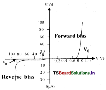
Forward bias – Threshold voltage (V0)
Threshold voltage is the voltage in a forward bias biased p-n junction at which the current suddenly rises to a large values.
The curve shows that the diode Conducts electric current during the forward bias but can not conduct during the reverse bias. Due to this property, diode is used as a rectifier.
Reverse bias – Breakdown voltage (VB)
Breakdown voltage: It is the voltage in a reverse biased p-n junction at which the current suddenly rises to a larger values.
Question 5.
Describe how a semiconductor diode is used as a half wave rectifier.
Answer:
Rectification: The process of converting alternating current (AC) into direct current (DC) is called rectification.
Half Wave Rectifier: A circuit which rectifies half of the AC wave is called Half wave rectifier.
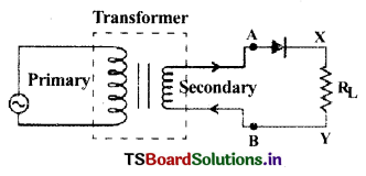
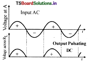
Diode as a Halfwave Rectifier: A single diode is connected in series to a load resistance RL in the secondary circuit of a transformer.
Working:
- During the positive half cycle, the diode is forward biased and the current flows through the diode.
- During the negative half cycle, the diode is reverse biased and the current does not flow through the diode.
- Thus, half wave is rectified using a single diode.
- Efficiency of Halfwave rectifier η = \(\frac{0.406 R_L}{r_f+R_L}\)
- Maximum Efficiency of Halfwave rectifier is 40.6%
Question 6.
What is rectification? Explain the working of a full wave rectifier.
Answer:
Rectification: The process of converting alternating current (AC) into direct current (DC) is called rectification.
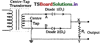
Full Wave Rectifier: The circuit which rectifies both half cycles of an AC wave is called Full Wave Rectifier.
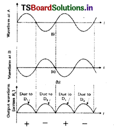
Working:
- During the first half cycle, the voltage on positive. It acts as forward bias. Hence current passes through RL. During this cycle, D2 is reverse biased. Hence no current passes through D2.
- During šecond half cycle, the D2 is forward biased and D1 is reverse biased. Hence, current passes through RL.
- Thus the full Wave is rectified using two diodes.
- Efficiency of full wave rectifier is η = \(\frac{0.812 R_L}{r_f+R_L}\)
Here rf = diode forward resistance, RL = load resistance. - Maximum Efficiency of full-wave rectifier is 81.2%
VI. Long Answer Questions
Question 1.
What is a junction diode ? Explain the formation of depletion region at the junction. Explain the variation of depiction region in forward and reverse-biased conditions.
Answer:
p-n junction Diode.The device having a p-n junction is called p-n junction diode.
The region where p-type and n-type semiconductors in contact is called p-n junction.
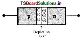
The symbol of p-n junction diode:
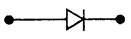
Depletion Layer: In a p-n junction diode, the electrons of n-side and holes of p-side diffuse to opposite sides and form a depletion layer at p-n junction. It is called so because, the free charge carriers are depleted from the region. The thickness of depletion layer is about one tenth of a micrometer.
Forward Bias: If a battery is connected to junction diode such that its positive terminal is towards p-end and its negative terminal is towards n-end, the diode is said to be in forward bias.
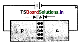
In forward bias, the applied voltage overcomes the barrier potential because the applied potential is greater and opposite to barrier potential. As a result, the width of the depletion layer decreases. The charge carriets can easily cross the depletion layer and a current passes through the diode.
Reverse Bias: If a battery is connected to a junction diode such that its positive terminal is towards n-end and its negative terminal is towards p-end, the diode is said to be in reverse bias.
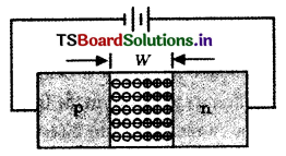
In reverse bias, the applied voltage cannot overcome the barrier potential because the applied potential is along the barrier potential. As a result, the width of the depletion layer increases. The charge carriers can not cross the depletion layer and no current passes through the diode.
Question 2.
What is a rectifier ? Explain the working of half wave and full wave rectifiers with diagrams.
Answer:
Rectifier: The device that converts AC into DC is called rectifier.
Rectification: The phenomenon of converting AC into DC is called rectification.
A) Half Wave Rectifier:
The half wave rectifier circuit is as shown in the figure. A single diode is connected in series to a load resistance RL in the secondary circuit of a transformer.
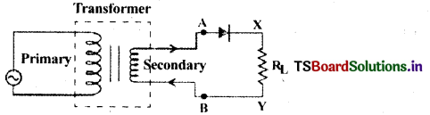
- As the current is AC, the direction of the current in the secondary winding changes after every half cycle.
- During the positive half cycle, the diode is forward biased and the current flows through the diode.
- During the negative half cycle, the diode is reverse biased and the current does not flow through the diode.
- The current through the load resistance is discontinuous pulsating DC as shown in the figure.
- The discontinuous pulsating DC can be made pure DC by using a filter circuit.
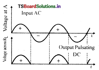
B) Full Wave Rectifier: The full wave rectifier circuit consists of two diodes (D1, D2), a load resistance (RL) in the secondary circuit of a centre tapped transformer as shown in the figure.
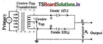
- As the current is AC, the direction of the current in the secondary winding of the transformer changes after every half cycle with respect to its centre tap C.
- During the first half cycle, the voltage on D1 is positive. It acts as forward bias to D1. Hence current passes to RL through D1. During this cycle, D2 is reverse biased. Hence no current passes through D2.
- During second half cycle, the D2 is forward biased and D1 is reverse biased. Hence, current passes to RL through D2.
- Thus the full wave is rectified.
- The output of full wave rectifier contains small variations as shown in the figure below. It can be made pure DC by using a filter circuit.
Exercise Problems
Question 1.
In a pure Intrinsic semiconductor, the number of conduction electron is 6 × 10¹⁹ per cubic meter. How many holes are there in a sample of size 1 cm × 2 cm × 2mm?
Answer:
Intrinsic concentration ni = 6 × 10¹⁹, m-3;
Volume v = 1cm × 2cm × 0.2cm = 0.4cm3 = 0.4 × 10⁻⁶m3
Total number of holes = ni × v = 6 × 1019 × 0.4 × 10-6 = 2.4 × 10¹³
Question 2.
Pure silicon at 300K has an equal number of electrons (ni) and the hole (nh) concentrations 5 × 10¹⁶ m-3. When it was doped with the indium then the hole concentration (nh) increases to 4.5 ×10²² m-3 then find the concentration of electrons after doping.
Answer:
Given ni = 5 × 10¹⁶m-3; nh = 4.5 × 10²²m-3
= 5.55 × 10¹⁰m3
Question 3.
An AC voltage with peak value 20 V is connected in series a diode and load resistance of 500Ω exists across the diode. Calculate the peak current through the diode and peak voltage across the load resistance when the diode is ideal.
Answer:
Given Vpeak = 20V, Resistance R = 500Ω
∴ Ipeak = \(\frac{V_{\text {peak }}}{R}\) = \(\frac{20}{500}\) = 0.04 = 40mA
Question 4.
A sample of pure silicon is doped with a trivalent impurity, where each impurity atom creates a hole. The concentration of holes in pure silicon is 7 × 10¹⁵ holes per cubic metre, and the density of silicon is 5 × 1028 atoms per cubic metre. The doping increases the hole conceñtration by a factor of 120. Calculate approximately the proportion in which the impurity is added.
Answer:
Given Initial concentration ni = 7 × 10¹⁵ m-3, Silicon density nSi= 5 × 1028 atoms/m3
Doping increase nh by a factor of 120
New hole concentration after doping nh = factor × ni = 120 × (7 × 1015) = 8.4 × 10¹⁷ holes / m3
No.of impurity atoms nim = 8.4 × 10¹⁷ atoms / m3
Proportion of impurity = \(\frac{\mathbf{n}_{\mathbf{S i}}}{\mathbf{n}_{\mathbf{i m}}}\) = \(\frac{5 \times 10^{28}}{8.4 \times 10^{17}}\) = 5.98 × 10¹⁰
Proportion of impurity = one in 5.98 × 10¹⁰ silicon atoms.
Question 5.
A potential barrier of 0.8V exists across the p-n junction. If the depletion region is 800 nm wide, then what is the intensity of electric field with in this region is?
Answer:
Barrier potential V = 0.8V
Width of depletion region d = 800 nm = 800 × 10-9 m = 8 × 10⁻⁷ m
∴ Electric field Intentisty E = \(\frac{V}{d}\) = \(\frac{0.8}{8 \times 10^{-7}}\) = 106 V/m
Question 6.
The diode shown in the circuit is a silicon diode, then find the potential difference between the points A and B ?
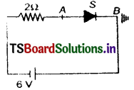
Answer:
Battery voltage V = 6V
Here, the diode is reverse bias. It acts as an open switch. No current flows through the circuit.
∴ The potential at A is VA = 6V. Also VB = 0
∴ The potential difference VAB = VA – VB = 6 – 0 = 6V
Question 7.
A diode having potential difference 0.7V across its junction which does not depend on current, is connected in series with resistance 100 ohms across source, if 0.1A passes through resistance. Then find the voltage of the source?
Answer:
Voltage drop across the diode Vd = 0.7V, Resistance R = 100Ω
Current in the circuit I = 0.1 A Voltage across R is VR = I × R = 0.1 × 100 = 10V
Source voltage Vs = Vd + VR = 0.7 + 10 = 10.7 V
Question 8.
A 2V battery is connected across AB as shown in the figure. The value of the current supplied by the battery when in one case battery’s positive terminal is connected to A and in another case when the positive terminal of the battery is connected to the B will respectively be?
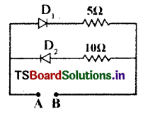
Answer:
Terminal A : Diode D1 is forward biased. So, current flows through 5Ω resistor
∴ current I1 = \(\frac{\mathrm{V}}{\mathrm{R}_1}\) = \(\frac{2}{5}\) = 0.4A
Terminal B :Diode D2 is forward biased So, current flows through 10Ω resistor
∴ current I2 = \(\frac{\mathrm{V}}{\mathrm{R}_2}\) = \(\frac{2}{10}\) = 0.2A
Question 9.
The I-V characteristics of a p-n junction diode in forward bias are shown in the following figure. Find the ratio of dynamic resistance corresponding to forward bias voltages of 2V and 4V?
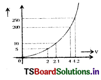
Answer:
(i) Dynamic resistance at 2V voltage
Voltage at V1 = 2V; current I1 = 5mA
Voltage at V2 = 2.1V; current I2 = 10mA
∴ ΔV = V2 -V2 = 2.1 – 2 = 0.1 V
ΔI = I2 – I1 = 10 – 5 = 5 × 10⁻³A
Resistance Rd1 = \(\frac{\Delta \mathrm{V}}{\Delta \mathrm{I}}\) = \(\frac{0.1}{5 \times 10^{-3}}\) = 20Ω
(ii) Dynamic resistance at 4V voltage.
Voltage at V3 = 4V, current I3 = 200mA
Voltage at V4 = 4.2V, current I4 = 250mA
ΔV = V4 – V3 = 4.2 – 4 = 0.2V
ΔI = I4 – I3 = 250 – 200 = 50 = 50 × 10-3A
Resistance R d2 = \(\frac{\Delta \mathrm{V}}{\Delta \mathrm{I}}\) = \(\frac{0.2}{50 \times 10^{-3}}\) = \(\frac{200}{50}\) = 4Ω
∴ Ratio = \(\frac{\mathrm{Rd}_1}{\mathrm{Rd}_2}\) = \(\frac{20}{4}\) = 5 : 1
Question 10.
Two ideal diodes are connected in the network as shown ¡n the figure. Then find the equivalent resistance
between A and B?
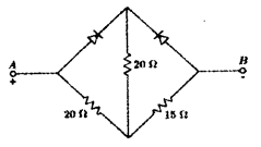
Answer:
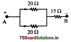
20Ω resistors are in parallel,
∴ \(\frac{1}{R_P}\) = \(\frac{1}{20}\) + \(\frac{1}{20}\) = \(\frac{2}{20}\) = \(\frac{1}{10}\) ⇒ RP = 10Ω
Equivalent resistance Req = RP + 15Ω = 10 + 15 = 25Ω
Question 11.
In the given circuit the diodes are IDEAL, then find the total resistance of circuit and the current reading in the ammeter.
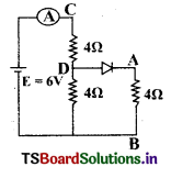
In parallel combination, \(\frac{1}{R_P}\) = \(\frac{1}{R}\) + \(\frac{1}{R}\) = \(\frac{1}{4}\) + \(\frac{1}{4}\) = \(\frac{2}{4}\) = \(\frac{1}{2}\) ⇒ Rp = 2Ω
Rtotal = Rp – 4 = 2 + 4 = 6 ;Voltage V = 6V and Rtotal = 6Ω
∴ Current I = \(\frac{V}{R}\) =\(\frac{6}{6}\) = 1A
Question 12.
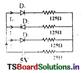
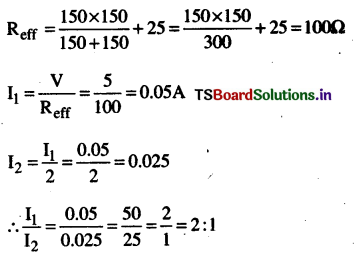
If each diode has a forward bias resistance of 25 ohms in the given circuit, then find the value of \(\frac{I_1}{I_2}\).
Answer:
In the figure diode D2 is in reverse bias.
So current does not flow. Thus I3 = 0
Objective Questions
Question 1.
When a triode is used as an amplifier the phase difference between the input signal voltage and the output is
1) 0
2) π
3) π/2
4) π/4
Answer:
2) π
Question 2.
In semiconductors at a room temperature
1) the valence band is partially empty and the conduction band is partially filled
2) the valence band is completely filled and the conduction band is partially filled
3) the valence band is completely filled
4) the conduction band is completely empty.
Answer:
1) the valence band is partially empty and the conduction band is partially filled
Question 3.
At absolute zero, Si acts as
1) non metal
2) metal
3) insulator
4) none of these.
Answer:
3) insulator
Question 4.
If a small amount of antimony is added to germanium crystal
1) it becomes a p-type semiconductor
2) the antimony becomes an acceptor atom
3) there will be more free electrons than holes in the semiconductor
4) its resistance is increased,
Answer:
3) there will be more free electrons than holes in the semiconductor
Question 5.
In a p type semiconductor, the majority carriers of current are
1) protons
2) electrons
3) holes
4) neutrons
Answer:
3) holes
Question 6.
Which of the following, when added us an impurity into the silicon produces n type semiconductor?
1) B
2) Al
3) P
4) Mg
Answer:
3) P
Question 7.
To obtain a p-type germanium semiconductor, it must be doped with
1) indium
2) phosphorus
3) arsenic
4) antimony.
Answer:
1) indium
Question 8.
When arsenic is added as an’ impurity to silicon, the’ resulting material is
1) n-type conductor
2) n-type semiconductor
3) p-type semiconductor
4) none of these.
Answer:
2) n-type semiconductor
Question 9.
When n type semiconductor is heated
1) number of electrons increases while that of holes decreases
2) number of holes increases while that of electrons decreases
3) number of electrons and holes remain same
4) number of electrons and holes increases equally.
Answer:
4) number of electrons and holes increases equally.
Question 10.
The increase in the width of the depiction region in a p-n junction diode is due to
1) forward bias only
2) reverse bias only
3) both forward bias and reverse bias
4) increase in forward current
Answer:
2) reverse bias only
Question 11.
In a p-n junction
1) high potential at n side and low potential at p side
2) high potential at p side and low potential at nside
3) p and n both are at same potential
4) undetermined.
Answer:
1) high potential at n side and low potential at p side
Question 12.
Depletion layer consists of
1) mobile ions
2) protons
3) electrons
4) immobile ions
Answer:
4) immobile ions
Question 13.
The depletion layer in the p-n junction region is caused by
1) drift of holes
2) diffusion of charge carriers
3) migration of impurity ions
4) drift of electrons.
Answer:
2) diffusion of charge carriers
Question 14.
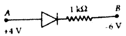
Consider the junction diode as ideal. The value of current flowing through AB is
1) 10-1 A
2) 10-3 A
3) 0 A
4) 10-2 A
Answer:
4) 10-2 A
Question 15.
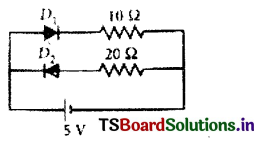
Two ideal diodes are connected to a battery as shown in the circuit. The current supplied by the battery is
1) 0.75 A
2) zero
3) 0.25 A
4) 0.5 A
Answer:
4) 0.5 A
Question 16.
Barrier potential of a p-n junction diode does not depend on
1) diode design
2) temperature
3) forward bias
4) doping density
Answer:
1) diode design
Question 17.
In forward bias, the width of potential barrier in a p-n junction diode
1) remains constant
2) decreases
3) increases
4) first (1) then (2)
Answer:
2) decreases
Question 18.
In a junction diode, the holes are due to
1) extra electrons
2) neutrons
3) protons
4) missing of electrons
Answer:
4) missing of electrons
Question 19.
The cause of the potential barrier in a p-n junction diode is
1) depletion of negative charges near the junction
2) concentration of positive charges near the junction
3) depletion of positive charges near the junction
4) concentration of positive and negative ch near the junction.
Answer:
4) concentration of positive and negative ch near the junction.
Question 20.
The peak voltage in the output of a half wave diode rectifier fed with a sinusoidal signal without filter is 10 V. The d.c. component of the output voltage is
1) 10/\(\sqrt{2}\)
2) 10/πV
3) 10 V
4) 20/π V
Answer:
2) 10/πV
Question 21.
If a full wave rectifier circuit is operating from 50 Hz mains, the fundamental frequency in the ripple will be
1) 25 Hz
2) 50Hz
3) 70.7 Hz
4) 100Hz
Answer:
4) 100Hz
Question 22.
A p-n junction diode can be used as
1) condenser
2) regulator
3) amplifier
4) rectifier
Answer:
4) rectifier
Question 23.
A Zener diode, having breakdown voltage equal to 15V, is used in a voltage regulator circuit shown in figure. The current through the diode is
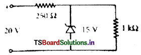
1) 5 mA
2) 10 mA
3) 15 mA
4) 20 mA
Answer:
1) 5 mA
Question 24.
A p-n photodiode is fabricated from a semiconductor with a band gap of 2.5 eV. It can detect a signal of wavelength
1) 4000 mn
2) 6000nm
3) 4000 A°
4) 6000 A°
Answer:
3) 4000 A°
Question 25.
Zener diode is used for
1) amplification
2) rectification
3) stabilisation
4) producing oscillations in an oscillator
Answer:
3) stabilisation
Question 26.
In the combination of the following gates the output Y can be written in terms of inputs A and B as
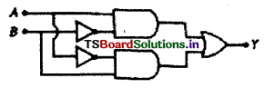
1) \(\overline{\mathrm{A} . \mathrm{B}}\)
2) \(\text { A. } \overline{\mathrm{B}}+\overline{\mathrm{A}} . \mathrm{B}\)
3) \(\overline{\mathrm{A} . \mathrm{B}}\) + A.B
4) \(\overline{A+B}\)
Answer:
2) \(\text { A. } \overline{\mathrm{B}}+\overline{\mathrm{A}} . \mathrm{B}\)
Question 27.
The given electrical network is equivalent to

1) OR gate
2) NOR gate
3) NOT gate
4) AND gate
Answer:
2) NOR gate
Question 28.
For the given circuit, the input digital signals are applied at the terminals A, B and C. What would be the output at the terminal y?
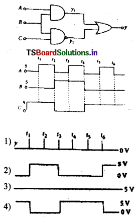
Answer:

Question 29.
What is the output Y in the following circuit, when all the three inputs A, B, C are first 0 and then I?
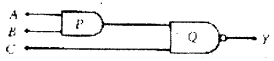
1) 0, 1
2) 0, 0
3) 1, 0
4) 1, 1
Answer:
3) 1, 0
Question 30.
The figure shows a logic circuit with two inputs A and B and the output C. The voltage wave forms across A, B and C are as given. The logic circuit gate is
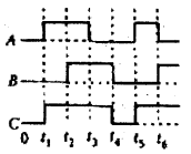
1) OR gate
2) NOR gate
3) AND gate
4) NAND gate
Answer:
1) OR gate
Question 31.
Symbolic representation of four logic gates are shown as
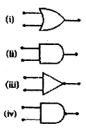
Pick out which ones are for AND, NAND and NOT gate, respectively
1) (ii), (iii) and (iv)
2) (iii), (ii) and (i)
3) (iii), (ii) and (iv)
4) (ii), (iv) and (iii)
Answer:
4) (ii), (iv) and (iii)
Question 32.
The device that can act s a complele electron k circuit is
1) junction diode
2) integrated circuit
3) junction transistor
4) zener diode.
Answer:
2) integrated circuit
Question 33.
The following truth-table belongs to which one of the fo1loin tour gates?
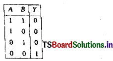
1) XOR
2) NOR
3) OR
4) NAND
Answer:
2) NOR
Question 34.
This symbol represents
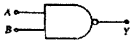
1) AND gate
2) NOR gate
3) NAND gate AB
4) OR gate
Answer:
3) NAND gate AB
Question 35.
The following truth table corresponds to the logical gate
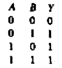
1) NAND
2) OR
3) AND
4) XOR
Answer:
2) OR